|
AAT's Information about Firm nanotools (Germany) Home Page Top  What's new!nanotools What's new!nanotools
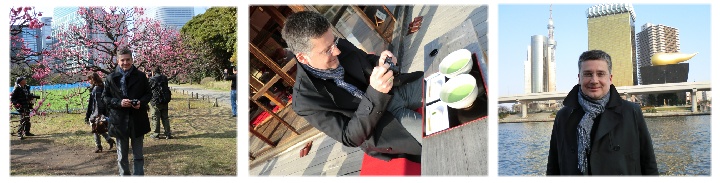
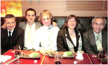
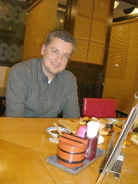
Last Updated : March 2012 Sightseeing in Tokyo with Dr. Irmer, who visits with business trip to Japan Dr. Bernd Irmer, President of Firm nanotools visited to Japan at the end of February. He had already visited the cutomer but he was tired because of the snowy day. On March 3rd, Saturday it was a nice weather and we took a stroll under the Winter sunshine in Tokyo, as from hotel, East Garden of the Imperial Palace, fountain near he Palace Hoel under construction, Tokyo Tower, Hamarikyu Reward Garden with Japanese apricot with red blossoms, Tee ceremony service in Chashitsu, Sumidagawa river-cruise and so on. Of course we could see the Tokyo Sky Tree waiting the opening ceremony in Spring.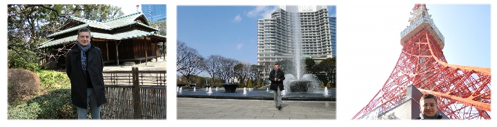
Last Updated : December 2011 From the nanotools' renewed HP we made a nanotool's pamphlet in English.
Last Updated : February 2011 Dr. Bernd Irmer, nanotools' President visits at nanotech 2011 and the nanotools' renewed HP
Last Updated : December 2009 Dr. Bernd Irmer, nanotools' President visits at Semicon Japan 2009
Last Updated : December 2008 Help to Firm nanotools' booth of German Pavillon in Semicon Japan 2008 From December 3, Wednesday to 5, Friday there is the show "Semicon Japan 2008". Firm nanotools exhibits at German Pavillon in No. 7 hall. However there is the show "2008 MRS Fall Exhibit" organized by the Materials Research Society in Boston, USA from December 2, Tuesday to 4, Thursday. President, Dr. Irmer and Ms Martin go to there. We help by oyeserlves at the nanotools booth. We made special posters called "AFM and Cantilever" whose photos were given by Firm Olympus. 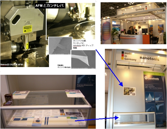
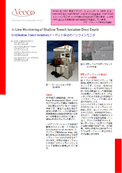
Last Updated : June 2008 Application Note AN99 by Firm Veecoeeco in 2007 was translated into Japanease.
Last Updated : December 2007 Help to Firm nanotools' booth in Semicon Japan 2007 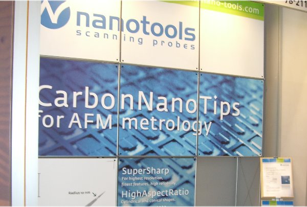 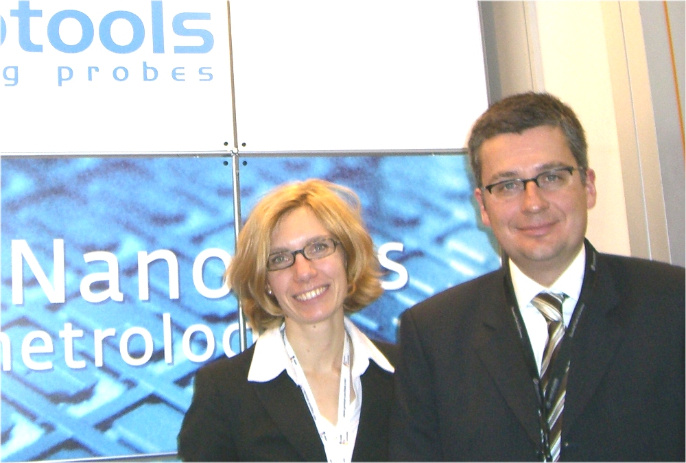 
From December 5, Wednesday to December 7, Friday the Semicon Japan2007 was held. Firm nanotools participated in German Paviilion at Hall 7. Ms Susanne Martin was coming one day before. This time the big banners was not used as the background of the booth, then the knockdown background was used and Ms Martin and I assembled it. The assembling frames and Photos are stored in 2 portable cases. This year 13 companies including nanotools were participated in German Pavilion and a customarly party organized by the Embassy of F.R. Germany was held at VIP room in Makuhari Messe in the evening of December 6 and we had friendly relations with other German companies. On the last day Dr. Bernd Irmer, CEO of nanotools GmbH, was coming to the show and made sales campaign by visiting other booths.
Last Updated : October 2007 Firm nanotools celebrated the 10th Anniversary of the Foundation at the main office in Munich on October 2, 2007 On Tuesday of October 2, 2007 Firm nanotools celebrated the 10th Anniversary of the Foundation with employee, managements and distributors of the world at his main office in Munich, Germany.We were also invited by Dr. Irmer, CEO of nanotools but unfortunately we had to stay in Japan because of the important business and we celebrated the 10th Anniversary far from Japan.
Last Updated : December 2006 Help to Firm nanotools' booth in Semicon Japan 2006 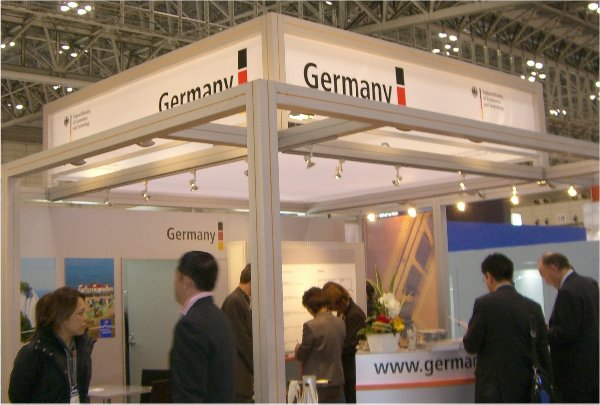 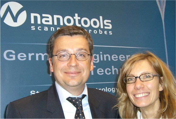 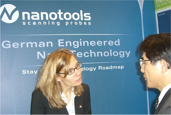 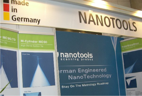 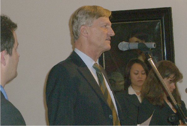 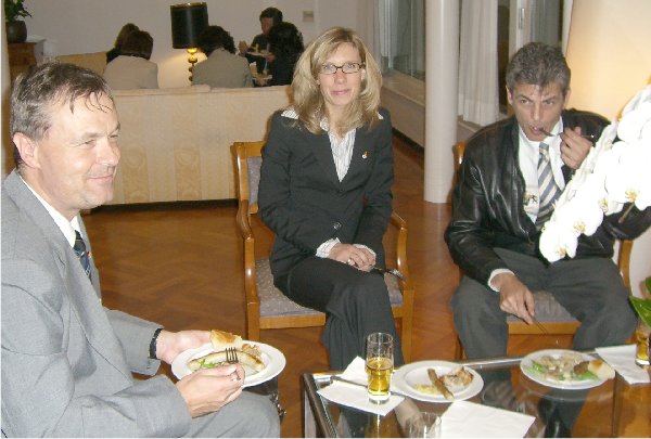
The Semicon Japan 2006 was held at Makuhari Messe from December 6, Wednesday to December 8, Friday 2006. Firm nanotools participated in German Pavilion at Hall 7. Ms Susanne Martin was coming one day before and advised the booth decoration. She brought some banners advertising nanotools' new products from Germany and decorated the booth using these banners and big banners prepared in Japan. Ms Martin could give a reception to visitors, so we were helper but we have only few helped. At the night of 1st day all participants in German Pavilion were invited to the official residence of Mr. Hans-Joachim Daerr Japanese Ambassador to F.R.Germany and enjoyed that night very much. On the last day of the exhibition Dr. Bernd Irmer, CEO of nanotools GmbH, was coming and made sales campaign.
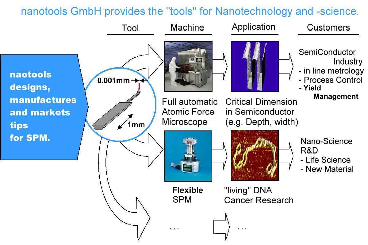
Last Updated : April 2006 Firm nanotools' booth in Semicon Europe 2006, Sales attack to the semi-conductor industries 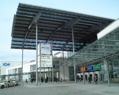 The semi-conductor industries using Automatic AFM in the production lines is the main market for Firm nanotools GmbH. The nanotools' tip is produced by an electric beam induced deposition (EBD) using the amorphous carbon technology.
The Semicon Europe 2006 was held at the trade Fair Center in Munich, Germany from April 4, Tuesday to 6, Thursday 2006 and Firm nanotools showed new tips with cylindrical shape for the AFM tip solution for 90nm, 65nm and 45nm in-line metrology. Then Dr. Irmer, CEO of Firm nanotools GmbH, had a lecture about "AFM tips for the Nano-electronics Research" at the MEMS Forum on April 4 of the same Trade Fair Center. The photo shows the entrance of the show. The photos bellow show the nanotools booth and new products were Metrology tips called M-Cylinder and M1. The former tip has a cylindrical shape with the minimum length of 600nm and the diameter of 55nm, and the latter one has a high aspect ration of 1:7 and is used at the in-line monitoring of a semi-conductor factory. 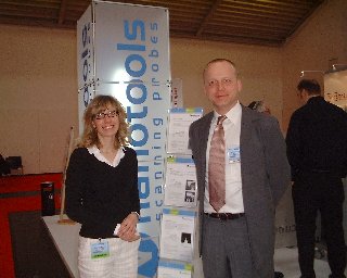
The upper left is M-Cylinder and the upper right is M1. Please refer to the following PDF-files about the detail.
Last Updated : November 2005 CNT-like M-Cylinder Cantilever for 90-70nm Node 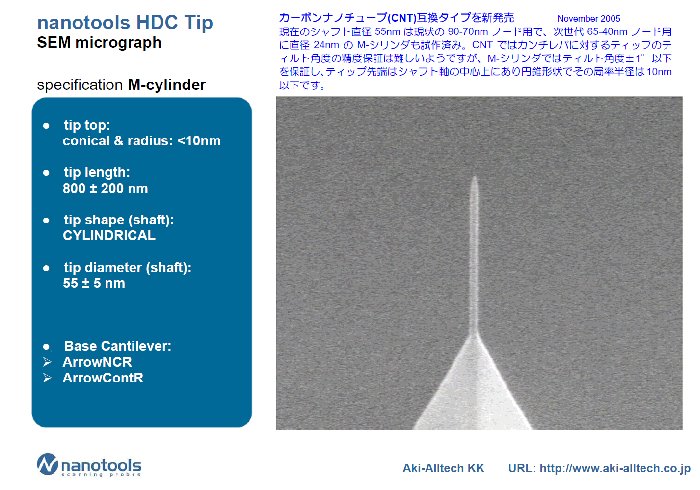
Last updated : March 2005 The equipment was reinforced, business is increasing, and Nanotools GmbH is getting bigger. 
 Recently we are often asked about cantilevers. The age of nanotechnology has begun and the number of customers who use SPM (scanning probes microscopes) is increasingly high. That's the point why we think that the interest in cantilevers is getting higher everyday. It is really important for us to get to know our customers' needs and questions as good as it gets. We consult with Nanotools and try to find the best advice and the best solution to offer.
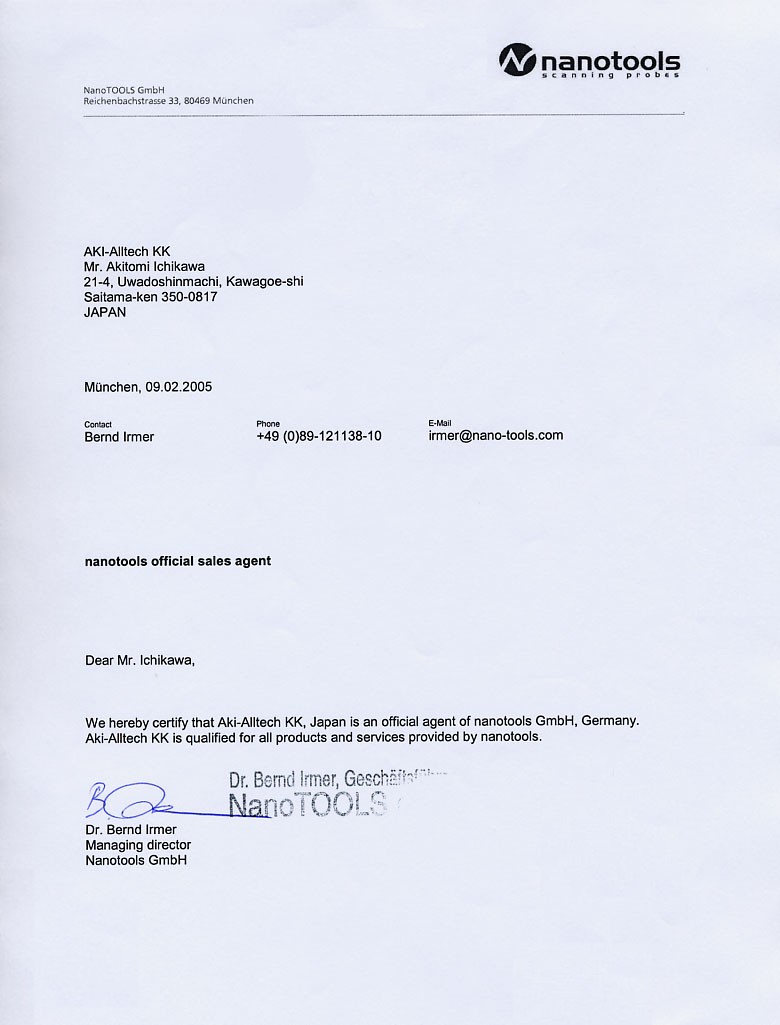
Here you can find the certificate of Nanotools' official agent, Dr.Irmer. (If you click on the certificate, you can see an enlargement.) A technical note on "Probe's knowledge to use the AFM well" in Japanese is being prepared. If you want you can ask for this document by E-mail.  Please ask us about technical information (only in Japanese) per E-mail. Please ask us about technical information (only in Japanese) per E-mail.
Last Updated : March 2004
 Please ask us about new English Image Catalogue with E-mail ! Please ask us about new English Image Catalogue with E-mail !
Last Updated : January 2004
Firm nanotools GmbH, Germany is the manufacturer of HDC(High Dense Carbon)-probes for AFM (Atomic Force Microscope) called a cantilever. This company was founded in 1997 as a spin-off of the Center for Nanoecience (CeNS) in Munich, bringing the technology which enabled to manufacture tips of almost any desired geometry and functionality. The nanotools modifies the tip and deposits the "HDC" material to the very end of the conventional silicon sensors as Nanosensors, Nanoworld, Olympus and Veeco's. Please refer to the following PDF-files about "Quick selection for HDC-tips", "Production list for HDC-tips" and "Applicatin samples of HDC-tips". 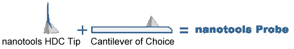 Import and Sales HDC-tips for SPM of Firm nanotools GmbH 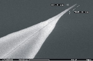
Last Updated : December 2003 At the end of November we visited 4 companies in Germany as Klocke Nanotechnik, Wilh. Lambrecht GmbH, Kappa opto-electronics GmbH and nanotools GmbH. We had meaningful meetings with them and we want to use theses experiences to support customers. nanotools GmbH : which was founded in 1997 as a spin-off of the Center for Nanoscience (CeNS) in Munich. As one research result of HDC (High Dense Carbon) technology they can manufacture a tip, which is used for AFM probes, and the tip is made to any desired geometry and functionality.  Not only in Japan but also in the World a nano-technology has met the prosperity right now, the sales amount of the HDC tips are growing up every year. Last year they moved to the center of Munich city from the CeNS site of Munich University. The office is near the Marienplatz, which is very famous place for Japanese tourists and in which there is new City Hall. The office has manufacturing and inspection facilities in basement, but there is no vibration effect from the metro. At the front of the nantools' poster by main entrance the right is Dr. Irmer ; CEO and the left is Mr. Kriele ;Managing Director Product Development. Not only in Japan but also in the World a nano-technology has met the prosperity right now, the sales amount of the HDC tips are growing up every year. Last year they moved to the center of Munich city from the CeNS site of Munich University. The office is near the Marienplatz, which is very famous place for Japanese tourists and in which there is new City Hall. The office has manufacturing and inspection facilities in basement, but there is no vibration effect from the metro. At the front of the nantools' poster by main entrance the right is Dr. Irmer ; CEO and the left is Mr. Kriele ;Managing Director Product Development.Each machine for inspection and manufacturing is operated and there are still manufacturing facilities in CeNS. They are planning to install one machine for manufacturing here in this office next year. They are ready to deliver the standard tips in Germany within 48 hours. They have renewed the company logo and homrpage recently. We have also sold tips to Japanese customers and we want to expand this business this year.
Last Updated : February 2003 December 2002 : Negotiation with Firm NanoTOOLS At the beginning The NanoTOOLS GmbH is specialized company to manufacture High Density Carbon scanning probes (HDC) for Atomic Force Microscopy (AFM). The NanoTOOLS HDC-tips are at least comparable to the tips made by best silicon AFM sensors with diamond coated. Furthermore the NanoTOOLS HDC-tips can be made to almost every geometry requested by customers, ranging from 100 nm short to well over 5 µm long needles, with tip radii from a very few nanometers to some 100 nm. Even more complex sensors, e.g. hook like tips, curved needles, closed loops to name but a few, can be made upon request. Whatever your need for a tool on the nanometer length scale might be, HDC material can well be the material you are looking for. Properties The NanoTOOLS HDC-tips are deposited onto a wide range of different types and materials of cantilevers, including the well known POINTPROBE silicon sensors from Nanosensors GmbH (The Nanoworld AG, Switzerland, acquired the Nanosensors GmbH in November 2002.), the world leader in silicon scanning probes, OLYPMUS Tapping Mode etched silicone probes, Park-Cantilevers and silicon nitride probes (contact, tapping in fluids). Advantages One of Applications
| |||||||||||||||||||||||||

 The nanotools' President, Dr. Irmer is interested in Japanese furnitures and garden. He had made Shoji directed by a Japanese lived in Munich, Germany. This time he wanetd to buy Kanna (Plane) and we went to a famous shop "Nishikan Honnten" durling the show. He bought a hand-made and an expensive real Kannna.
 Firma nanotools makes Image Catalogue in March 2004, which shows Company policy, products, solutions and so on. We can prepare also the Image Catalogue in Japanese.
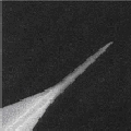
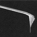

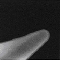
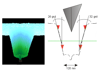 Deep DRAM-trench analyzed with a commercial silicon-tip
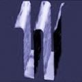
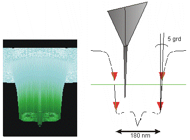 The same DRAM-structure analyzed with a NanoTOOLS HDC Metrology AFM tip.