|
Support für Firma nanotools (Deutschland)
Homepage Top Service & SupportSupport für nanotools Service & SupportSupport für nanotools
Wir haben keine Zeit, um Information auf Englisch ins Deutsche zu übersetzen. Entschuldigung !
FAQ about Firm nanotools, their Products and Terminology
|
Answers of the FAQ (Frequently Asked Questions) |
- What is AFM and/or cantilever ?
(Answer)
We describe briefly about AFM. AFM means Atomic Force Microscopy and the extension of SPM (Scanning Micro Scopy), which is a technique consisting of a probe with a measuring device to analyse the small vertical movement as it travels over a sample. When the probe scans over the sample, the computer controlled feed-back system maintains a constant interaction between the stylus of the probe and sample surface. The AFM uses the constant atomic force between the probe and sample surface. The idea of the AFM is combined the principle of the STM (using constant electron tunnelling) and a Styus profilometer. An AFM consists of a silicon conicial probe with a 10nm in radius and this probe is mounted on a low spring constant cantilever arm. The tip follows the surface contour and the computer uses constant force to maintain the distance by feed back.
- What is EBD ?
(Answer)
EBD means Electron Beam Deposition and is a technique to transport a high-energy and high current beam of electrons to a target through a vacuum, and create an impact of evaporant material of a gas molecules on a substrate to produce a finished deposition.
- What is the material, hardness and a lifetime of HDC-tip ?
(Answer)
The HDC material consists mainly of an amorphous carbon matrix including diamond or metal like nano-crystallites. There are no reliable hardness data because of the nanometer scale, instead we can give the Young modules (Gpa). Diamond is 1400 Gpa, Silicon is 107 Gpa and HDC is 770 Gpa. It means that hardness is comparable to that of diamond, but not brittle like silicon material. We can say a lifetime is semipermanent.
- What is the geometry like cone half angle, aspect ration and so on ?
(Answer)
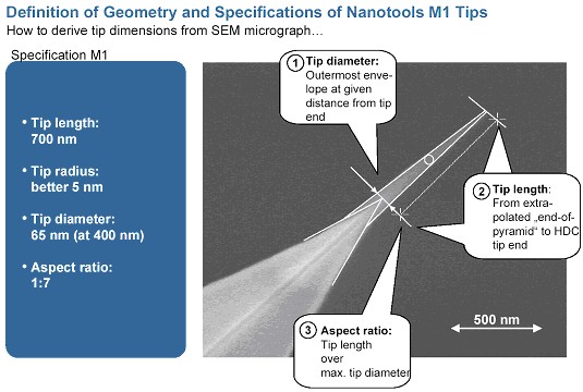
The cone anle means a half of a tip angle formed by tip radius. The above picture shows the definition of some words.
- What means hydrophobic ?
(Answer)
HDC is hydrophobic means that the interaction between the HDC-tip and the sample is so weak. You can use HDC-tip in acid liquids and/or basics liquids. If you use the hydrophil tip (e.g. silicon tip with their natural oxide coating) would end in a huge water bubble between tip and sample.
- What means degradation ?
(Answer)
Degradation means wear, breaking apart - whatever damages tip. Most common is wear.
- Can you issue the test certificate ?
(Answer)
We have the option of issuing the certificate which shows length, diameter, tip radius and tilt angle. Every electron imaging system in general does contaminate the sample under investigation, even those working under very high vacuum conditions. The HDC-tip itself can become easily and very rapidly be contaiminated.(*) In most cases this changes the geometry and its unique material properties so drastically that it is not a "real" HDVC-tip anymore. We therefore must give strong advice against any imaging in electron microscope systems. For our certificates, i.e. high resolution images, we use a modified SEM working under inert gas atmosphere and ultra high vacuum conditions in combination with low electron energies. Only this imaging conditions guarantee a non destructive imaging process.
(*) Please refer to the information "Knowledges about Probe to use AFM well." in Japanese from Aki-Alltech KK.
- What we have to pay attention to handle EDB-tips ?
(Answer)
Information on using and handling EBD-probes:
EBD probes are custom-made, individually manufactured and certificated AFM probes. They are characterised by outstanding resolution in combination with extreme durability and chemical stability. They can be used as any other AFM probe in all scanning applications. However, In order to obtain the best results, please note the following remarks on cleaning and scanning properties.
Cleaning
In normal scanning operation EBD probes do not tend to contaminate, since most materials adhere only very badly on EBD material. With particularly adhesive samples, or if the EBD probe deeply immerses into the sample like for example in lithography, some contamination might occure. In such cases we recommend to carefully immerse the probe into a solvent (e.g. water, acetone, alcohol,...) and dry blow it with compressed nitrogen or compressed air. EBD material is not attacked by most solvents. We strongly discourage you from using plasma cleaning or any physical etching, bacause some reactive plasma do indeed attack the EBD probes.
Behaviour in the AFM operation:
EBD probes are charaterised by the fact that they do not suffer or degrade under high loading forces (contrary to many other AFM probes). EBD material itself shows a hardness comparable to that of diamond but is also flexible to a certain degree. Therefore EBD-probes tend to elastically bend under very high loading forces. With long and highly sharpened tips this may lead to imaging artefacts, when scanned at high frequencies, low setpoints i.e. high loading forces and large scan sizes. By reducing the force on them, mainly by increasing the setpoint and readjusting the other scanning parameters, the tip will recover and show the initial superb imaging quality.
In general we advise to scan slower for longer tips.
Imaging in electron microscopes:
Every electron imaging system in general does contaminate the sample under investigation, even those working under very high vacuum conditions. The EBD tip itself can become easily and very rapidly be contaiminated. In most cases this changes the geometry and its unique material properties so drastically that it is not a "real" EBD tip anymore. We therefore must give strong advice against any imaging in electron microscope systems. For our certificates, i.e. high resolution images, we use a modified SEM working under inert gas atmosphere and ultra high vacuum conditions in combination with low electron energies. Only this imaging conditions guarantee a non destructive imaging process.
- What are the differences between HDC-tip and CNT-tip ?
(Answer)
 According to the information of Firm SII there are CNTs classfied roughly into 2 kinds, such as SWCNT (Single Wall CNT) and MWCNT (Multi Wall CNT). It is considered that MWCNT has inside several SWCNTs each other. The diameter (tip radius and thickness) of SWCNT is about 2nm, however this tip is coming from one point of the wall around, therefore this tip is not limited to come from the center axis of the wall. Then the mechanical strength is small to use in SPM, and so the application is limited. On the other hand the diameter of MWCNT is about 8-30nm. This tip is not sharp compared the Silicon Cantilever (Tip diameter of Super Sharp Tip is about 5nm), but the tip located in the center of the tube.
The CarbonNanoTip M-CNT, that is, the latest one of nanotools' EBD HDC-tips (Electron Beam Induced Deposition High Dense Carbon-tips) is developped from their Metrology-tip M-Cylinder, which is used already in the production lines for 90-70nm Node and whose specification is 55nm in shaft diameter and 600nm in minimum length. The M-CNT is 20nm in shaft diameter for the next generation of 65-40nm Node.In fact it is a high-aspect tip as the shaft diameter is 20nm and minimum length is 500nm. And then this tip nose is located on the shaft center axis and its nose radius is under 10nm. The tip length and the tip angle position in both direction can be controlled by the request of the und users.
- Summary about cantilever tip
(Answer)
 The EDB-tips are now 4 types according to each application, (1) trench, (2) super-Sharp, (3) lithography and (4) life science.
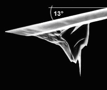
(1) The original probes (cantilevers) for the trench application are the ArrowNC and NCH from Firm NanoWorld and TEST from Firm Veeco.. The tip geometry is cone and the cone tip is tilted 13º or 3º with the tilting correction ۫· to the cantilever axis, so that the tip is normal to the sample surface. The cylinder shape tip is also available and the cylinder tip is tilted 13º or 3º with the tilting correction ۪.5· to the cantilever axis, in this case. In the case of the CNT-tip, the tilt angle adjustment is difficult because of the tip adhesion and the fixed length adjustment is also difficult because of the hard CNT and/or the hard control of the crystallization. In the case of the Silicon tip, the length adjustment is done but the tip cannot tilt because of the soft silicnon.
(2) The super-Sharp tip is used for the roughness measurement. The HDC-tip can be deposited on the soft probe of FMR from Firm NanoWorld. The tip geometry is cone and the cone tip is tilted 13º or 3º with the tilting correction ۫·. In the case of the CNT-Tip adhesion, it is said that the tilting correction is 䔸·.
(3) For the lithography application the big HDC-tip are available now.
(4) For the life science application the HDC-tip can be deposited on the probes from Firm Olympus in Japan. This is a general idea for the HDC-Tip deposition. This deposition is also possible on the cantilever of other types and the tilting angle pf tip is adjusted according to the customerfs requirements.
(5) For other Veecofs CD (Critical Dimension) application this tip geometry is very severe. The nanotoolsf former HDC-tip couldnft be deposited as top-heavy, but now he can. Then why CD-AFM is often used than SEM, then the sample must be cut in the SEM application but CD-AFM can measure a sample without cutting. It is said that the HDC-tip deposition is best using EBD technology.
|
 Benutzen Sie E-mail bitte, um uns Materialien zu fragen order uns Kommentare ze senden ! Benutzen Sie E-mail bitte, um uns Materialien zu fragen order uns Kommentare ze senden !

|